Global semiconductor sales are expected to fall 7.2 percent in 2019 as demand weakens amid a global memory slump, but emerging technologies such as wafers, chips and transistors are expected to bring innovation to the IC market.
At the Imec annual BBS Technology Forum (ITF) held in ANTWERP, Belgium, the proposed Technology will completely transform the traditional SoC System on a Chip, but in the future, there will be challenges in component calibration and cooling.
New version of SoC chip
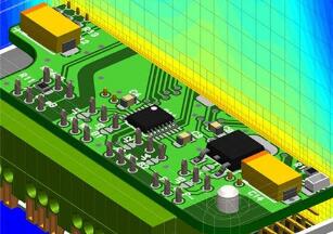
It is worth mentioning that the new SoC is expected to achieve power dissipation (thermals) of more than 500W.
Imec sequential 3D, as it has sequential 3D, this radically revised SoC structure, provides sequential upgrades and designs for a variety of different power supplies, logic chips and memory circuit boards.
In one version, power transfer circuits are placed on the back of wafers that have been sliced to a thickness of a few hundred nanometres, connected through tiny silicon vias.
Through - Silicon Vias, also called TSV, is a 3 d IC assembly follow the interconnection technology of Moore's law can be stacked multichip TSV chip, its design concept comes from the printed circuit board (PCB), drill a small hole in the chip, from the bottom of the filling into the metal, Silicon wafer by etching or laser drilling (Via), again with conductive materials such as copper, polysilicon, tungsten material filling.
Another bold option is to place an SRAM flash memory on top of the core circuit that carries the wafer, and copper to copper bonding.
The final sequence 3D will be a sandwich structure: the SRAM array at the bottom, the power circuit at the top, and the core logic sandwiched between
This maximizes SRAM while reducing costs.

The technology opens up more possibilities for integrating components, although Imec's original 5-nanometer demonstration did not include any active structures.
"This opens up a whole new field," said Julien Ryckaert, director of the logical process microscale project at Imec. "there will be a lot of technological blueprints for innovation, so Moore's law will continue to be implemented."
But as they progress to one or two nanometers, engineers will need to swap copper and cobalt, possibly using ruthenium, a material that allows wafer designers to thin metal barriers currently used to prevent the diffusion of metals into silicon oxides.
In addition to the chip process, the researchers also discussed packaging technologies, such as Imec's ongoing development of a "cheap version" of Intel's embedded multichip interconnect bridging technology (EMIB), which integrates bridging substrates into packaging.Other technological options include interconnections in the hundreds of microns and tens of nanometers.
Eric Beyne, a research fellow at Imec who is working on the 3D chip project, said the packaging blueprint still faces some gaps in device functionality, with dense layers of chips producing large amounts of power-dissipating components, liquid cooling methods still being developed, and EDA tools to support full nuclear signage not yet in place.
"But we've seen good progress."Beyne said.
Integration of old and new technologies
As Mike Mayberry, Intel's chief technology officer, noted in his keynote address, the innovations and innovations in chip technology represent the evolution, not the end, of traditional semiconductors.
Older processors will coexist with newer accelerators for specific domains, such as Microsoft's integration of x86 processors with FPGA in its data center.
At present, analysts are optimistic about the second half of 2019, the semiconductor market will have a strong development.Although current semiconductor sale falls, nevertheless the innovation of IC market suggests the market still has development potential.

 Inglés
  Chino
Chino  Alemán
  Coreano
  Japonés
  Farsi
Farsi  Portuguese
  Russian
  Español


